This is an old revision of the document!
Table of Contents
PCB Etching
Equipment
Safety
There is currently no access control on any of the PCB-specific equipment or substances. There probably should be.
UV exposer: currently it is unknown if this will switch on without the lid being closed. Do not be the person to find out.
Flux spray: use in the workshop, over a bin, with the ventilation on max. Wear eye protection.
Sodium carbonate (“washing soda”/photonegative developer): You can touch this, but you probably don't want to. Can be flushed down the drain.
Sodium hydroxide (“drain cleaner”/photonegative stripper): Highly caustic. Wear gloves. Can be flushed down the drain (it's drain cleaner).
Ferric chloride (etchant): Wear gloves. Wear eye protection. Touch it and die. Can be reused for months or even years, so you shouldn't need to dispose of it; if you do, there's a tub under the sink for the used stuff. DO NOT flush down the drain.
Design/file prep
Prepare your design using your PCB software of choice (KiCad is a good open-source option). Start with nice thick traces (at least 0.8mm) and then try going smaller once you've got the hang of the masking and etching process.
Export one file with your cuts and another with your circuit traces. If you're making a double-sided board, you'll need one trace image for each side, but double-sided boards are trickier right now (see notes under “Cutting” below). Note that KiCad doesn't actually export all through-holes on the “edge cuts” setting. You might find it easier to export a single image with your copper traces and “print board edges on all pages” ticked, then separate the traces/pads from the holes in Inkscape/Illustrator/etc.
Cutting
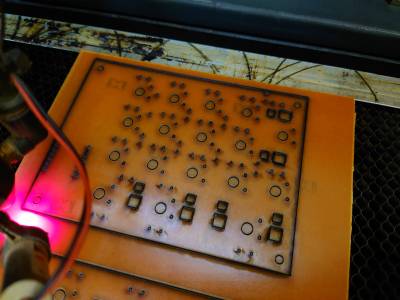
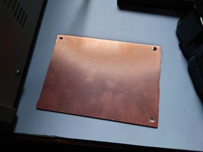
With the CNC router not really in working order at the moment, the best way to cut your board is with one of the laser cutters. This is subject to two major restrictions: use FR1 or FR2 boards ONLY (FR4 vapourises into some VERY nasty stuff), and use only single-sided boards (you can't laser through copper).
Use your image editing software of choice to prepare your cut file for lasering. It needs to be a vector with all shapes as outlines and no fill, and it needs to be mirrored either in your image editor or once you import it into the LaserCut software.
Place your workpiece in the laser cutter copper side DOWN. Cut settings may need some experimenting to get right. The aim is to cut all the way through the substrate without hitting the copper hard enough to cause lots of sparks. My best results have come from using the big laser with speed 35, power 60, corner power 50 on 1.5mm board.
Run the cuts. Give it a couple of minutes before you open the lid, vapourised FR1/2 isn't as bad as FR4 but it's still unpleasant.
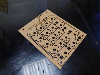
Take the workpiece out and pop your board out of it. What you're doing here is snapping the copper layer along the lines you've cut in the substrate, it'll be tough but doable. You may need to flex the board a bit. You can leave the through-holes for now, although you may find it useful to punch out any mounting holes to help you align the trace design in the exposure step. Note that you'll lose some copper around the edges of whatever you pop out, so only do this in non-critical areas of your board.
Exposure
Grab the laminator, some sellotape, and a pair of scissors from G1 before you start with this section.
Currently (as of January 2022) the lab has NEGATIVE photoresist, which means the copper will be removed from the areas of your board NOT exposed to UV light.
In the past the recommendation has been to use transparencies run off the laser printer for UV masking. This does not actually work very well because the “black” areas do not come out fully opaque. Tracing paper may work - as of this writing we don't have any. One good way to produce a UV mask in the absence of proper printables is to laser-cut your trace pattern into a scrap bit of very thin plywood or black acrylic.
Cut a piece slightly larger than your board from the roll of photoresist film kept wrapped in a black bag in the cabinet in G14. PUT THE ROLL BACK IN THE BAG - it's UV sensitive.
Peel off the backing (this is incredibly annoying to do - a couple of pieces of sellotape on either side of the corner can help peel the layers apart) and apply the blue film to your board. Try to squeeze any bubbles or wrinkles out to the sides, then run the board through the laminator. The laminator should be set on the largest thickness setting (2x125MIC), and it helps to run it through two or three times to improve the bond.
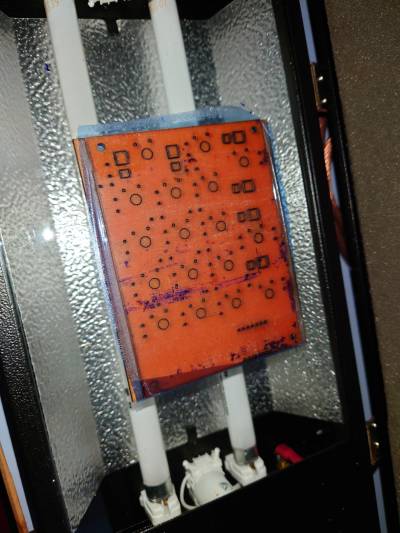
Put your mask and film-coated board together in a sort of deadly yet exciting chemical sandwich. Align as best you can using the mounting holes you hopefully punched out earlier, and add some sellotape to hold everything together.
Place your sandwich in the UV exposure box (aka the PCB panini press). Close the box and expose for ~1.5 minutes. After exposure the design may be visible on the PCB but can be hard to see.
Developing
This step removes any photoresist that has been exposed to UV light in the previous step.
Make a solution of about 500ml water and 20g washing soda crystals (sodium carbonate decahydrate). There is a handy 3D-printed scoop to help you get the right amount of washing soda.
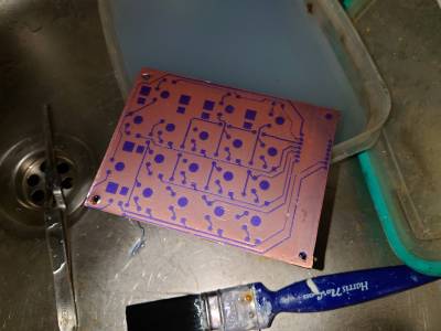
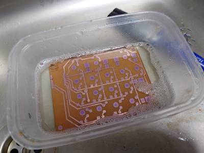
Immerse the PCB in the solution for a few seconds, then remove it. You should now be able to easily peel off the transparent film on the front. Return the board to the solution and start gently brushing it with the paintbrush. You should notice bits of the blue mask coming off. Once all the copper you want to remove is exposed (this should take about 30-60 seconds), remove from the solution and rinse with plenty of water.
If you're having trouble getting the unwanted film to come off, your board is overexposed. If your traces/pads are coming off too, it's underexposed. Either way, strip the film off using the instructions below and try again. Most likely you need to increase or decrease the time in the UV box.
Etching
Plug in and turn on the etch tank and give it some time to warm up.
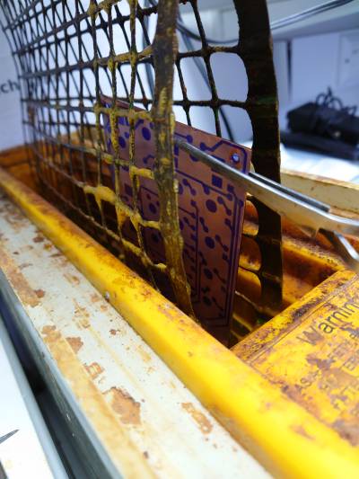
Put your PCB in the tank, using the net hanging from the lid to hold it so you can get it back out easily.
Check on it after a couple of minutes, by which time all copper to be removed should turn a dull pink. “Dull” is an important word here; you're looking for “barbequed pig”, not “rose gold”. If you get rose gold, the PCB is either under-exposed or under-developed. You can try rinsing the PCB with plenty of water and returning to the develop step for 10-20 seconds, before continuing with etching.
Your board is finished when all the unwanted copper is gone. This usually takes about 10 minutes. Start checking it every minute or two after it's been in for 10, and take it out when the unwanted copper has all dissolved leaving just the substrate underneath. If you hit 15 minutes, your board may be underdeveloped.
Once it's finished etching, turn off the etch tank and rinse the board with lots of water before touching it.
Stripping
This step removes the rest of the photoresist from the board. Pour some drain cleaner into a tray and soak your board in it for 15-30 minutes, agitating and scraping it every few minutes with the toothbrush.
Once all blue photoresist has been removed, you should see your copper traces. Rinse your board off with lots of water and pop out the remaining through holes, using a .5mm drill bit if needed.
Note: pure caustic soda will do the stripping job faster than regular commercial drain cleaner, hopefully we will be getting some in soon and this section can be updated.
Final checks
Inspect your board for any broken traces or traces/pads that haven't separated properly. Pads on microcontroller sockets are a notable culprit as they're often very close together and the masking process might not separate them fully.
Where two traces/pads have merged, you can remove some of the copper with a knife, sharp pair of tweezers, etc.
Where a trace has been broken, apply a solder bridge to reconnect it.
Flux
Give your new board a spray with the can of flux. This will both prevent the copper traces from oxidising and make soldering to the board easier. Applies just like spraypaint - use back-and-forth motions from 20-30cm away.
Leave to dry for a couple of hours. Congratulations, you made a PCB!!
